Interface Specifications
This section outlines the interface specifications for the SC-OBC Module A1 Module.
CON1 (IO Board Interface)
The IO Board interface connects the OBC Module and the IO Board. This interface uses a Panasonic 0.5 mm pitch 80-pin connector (model number: AXK6S80547YG). Use a socket with a mating height of 5 mm, 5.5 mm, or 8 mm to connect with the corresponding IO board.
Refer to the Board Layout Diagram for connector locations.
| Pin Number | Pin Name | I/O | Power Domain | Description |
|---|---|---|---|---|
1 |
VIN_A |
Power |
- |
Power supply (VIN_A) |
2 |
VIN_A |
Power |
- |
Power supply (VIN_A) |
3 |
VIN_A |
Power |
- |
Power supply (VIN_A) |
4 |
ULPI_DP |
Inout |
- |
SC Bus D + signal |
5 |
ULPI_DM |
Inout |
- |
SC Bus D - signal |
6 |
GND |
Power |
- |
Ground |
7 |
UIO1_00 |
Inout |
VDD_UIO1 |
User IO1 Bit 0 signal is connected to FPGA pin IO_L13P_T2_MRCC_34 (pin: R3). |
8 |
UIO1_01 |
Inout |
VDD_UIO1 |
User IO1 Bit 1 signal is connected to FPGA pin IO_L13N_T2_MRCC_34 (pin: P3). |
9 |
UIO1_02 |
Inout |
VDD_UIO1 |
User IO1 Bit 2 signal is connected to FPGA pin IO_L14P_T2_SRCC_34 (pin: P4). |
10 |
UIO1_03 |
Inout |
VDD_UIO1 |
User IO1 Bit 3 signal is connected to FPGA pin IO_L14N_T2_SRCC_34 (pin: N4). |
11 |
UIO1_04 |
Inout |
VDD_UIO1 |
User IO1 Bit 4 signal is connected to FPGA pin IO_L11P_T1_SRCC_34 (pin: M2). |
12 |
UIO1_05 |
Inout |
VDD_UIO1 |
User IO1 Bit 5 signal is connected to FPGA pin IO_L11N_T1_SRCC_34 (pin: L2). |
13 |
UIO1_06 |
Inout |
VDD_UIO1 |
User IO1 Bit 6 signal is connected to FPGA pin IO_L10P_T1_34 (pin: H2). |
14 |
UIO1_07 |
Inout |
VDD_UIO1 |
User IO1 Bit 7 signal is connected to FPGA pin IO_L10N_T1_34 (pin: H1). |
15 |
GND |
Power |
- |
Ground |
16 |
UIO1_08 |
Inout |
VDD_UIO1 |
User IO1 Bit 8 signal is connected to FPGA pin IO_L7P_T1_34 (pin: K1). |
17 |
UIO1_09 |
Inout |
VDD_UIO1 |
User IO1 Bit 9 signal is connected to FPGA pin IO_L7N_T1_34 (pin: J1). |
18 |
UIO1_10 |
Inout |
VDD_UIO1 |
User IO1 Bit 10 signal is connected to FPGA pin IO_L9P_T1_DQS_34 (pin: N1). |
19 |
UIO1_11 |
Inout |
VDD_UIO1 |
User IO1 Bit 11 signal is connected to FPGA pin IO_L9N_T1_DQS_34 (pin: M1). |
20 |
UIO1_12 |
Inout |
VDD_UIO1 |
User IO1 Bit 12 signal is connected to FPGA pin IO_L18P_T2_34 (pin: U2). |
21 |
UIO1_13 |
Inout |
VDD_UIO1 |
User IO1 Bit 13 signal is connected to FPGA pin IO_L18N_T2_34 (pin: U1). |
22 |
UIO1_14 |
Inout |
VDD_UIO1 |
User IO1 Bit 14 signal is connected to FPGA pin IO_L1P_T0_34 (pin: K3). |
23 |
UIO1_15 |
Inout |
VDD_UIO1 |
User IO1 Bit 15 signal is connected to FPGA pin IO_L1N_T0_34 (pin: J3). |
24 |
GND |
Power |
- |
Ground |
25 |
UIO3_00 |
Inout |
VDD_3V3_SYS / VDD_3V3_IO[1] |
Power domains differ depending on hardware options. See “Hardware options and IO connections” [fuzzy:*Hardware options and IO connections]. User IO3 Bit 0 signal is connected to RD4/PSP4 of the PIC16LF877. This can be reassigned to FPGA pin IO_L23P_T3_12 (pin: Y15) via hardware configuration options. |
26 |
UIO3_01 |
Inout |
VDD_3V3_SYS / VDD_3V3_IO[1] |
User IO3 Bit 1 signal is connected to RD5/PSP5 of the PIC16LF877. This can be reassigned to FPGA pin IO_L23N_T3_12 (pin: AA15) via hardware configuration options. |
27 |
UIO3_02 |
Inout |
VDD_3V3_SYS / VDD_3V3_IO[1] |
User IO3 Bit 2 signal is connected to RD6/PSP6 of the PIC16LF877. This can be reassigned to FPGA pin IO_L24P_T3_12 (pin: W14) via hardware configuration options. |
28 |
UIO4_00 |
Input |
VDD_3V3_IO |
User IO4 Bit 0 signal is connected to FPGA pin IO_L22P_T3_12 (pin: AB16). |
29 |
GND |
Power |
- |
Ground |
30 |
TRCH_UART_TX |
Output |
VDD_3V3_SYS / VDD_3V3_IO[1] |
TRCH UART TX signal is connected to RC6/TX/CK of the PIC16LF877. This can be reassigned to FPGA pin IO_L24N_T3_12 (pin: W15) via hardware configuration options. |
31 |
TRCH_UART_RX |
Input |
VDD_3V3_SYS / VDD_3V3_IO[1] |
TRCH UART RX signal is connected to RC7/RX/DT of the PIC16LF877. Using hardware options, it can be reassigned to FPGA IO_L1N_T0_12 (pin: AE26). |
32 |
VDD_3V3_SYS |
Power |
- |
Power supply (VDD_3V3_SYS) output |
33 |
GND |
Power |
- |
Ground |
34 |
I2C_EXT_SCL |
Output |
VDD_3V3_SYS |
I2C SCL signal connects the PIC16LF877 RD2 PSP2 pin to the FPGA IO_L9P_T1_DQS_12 pin at AE22. It is pulled up with a 4.7 kΩ resistor. |
35 |
I2C_EXT_SDA |
Inout |
VDD_3V3_SYS |
I2C SDA signal connects the PIC16LF877 RD3 PSP3 pin to the FPGA IO_L9N_T1_DQS_12 pin at AF22. It is pulled up with a 4.7 kΩ resistor. |
36 |
WDOG_OUT |
Output |
VDD_3V3_SYS / VDD_3V3_IO[1] |
Watchdog output signal is connected to RE0/AN5/RD of the PIC16LF877. It can be switched to FPGA IO_L16N_T2_12 (pin: AF18) via hardware options. |
37 |
VDD_3V3_IO |
Power |
- |
Power supply (VDD_3V3_IO) output |
38 |
VDD_3V3_IO |
Power |
- |
Power supply (VDD_3V3_IO) output |
39 |
VDD_UIO1 |
Power |
- |
Power supply (VDD_UIO1) |
40 |
VDD_UIO1 |
Power |
- |
Power supply (VDD_UIO1) |
| Pin Number | Pin Name | I/O Type | Power Domain | Description |
|---|---|---|---|---|
41 |
VDD_UIO2 |
Power |
- |
Power supply (VDD_UIO2) |
42 |
VDD_UIO2 |
Power |
- |
Power supply (VDD_UIO2) |
43 |
UIO4_05 |
Inout |
VDD_3V3_IO |
User IO4 Bit 5 / CM3 NTRST signal is connected to FPGA IO_0_13 (pin: U24). |
44 |
UIO4_04 |
Inout |
VDD_3V3_IO |
User IO4 Bit 4 / CM3 TDO and SWO signals are connected to FPGA IO_L16P_T2_13 (pin: W20). |
45 |
UIO4_03 |
Inout |
VDD_3V3_IO |
User IO4 Bit 3 / CM3 TDI signal is connected to FPGA IO_L16N_T2_13 (pin: Y20). |
46 |
UIO4_02 |
Inout |
VDD_3V3_IO |
User IO4 Bit 2 / CM3 TMS and SWDIO signals are connected to FPGA IO_L14N_T2_SRCC_13 (pin: Y21). |
47 |
UIO4_01 |
Inout |
VDD_3V3_IO |
User IO4 Bit 1 / CM3 TCK and SWCLK signals are connected to FPGA IO_L14P_T2_SRCC_13 (pin: W21). |
48 |
GND |
Power |
- |
Ground |
49 |
ICSP_PGD |
Inout |
VDD_3V3_SYS |
PIC PGD signal is connected to RB7 / PGD of PIC16LF877. |
50 |
ICSP_PGC |
Inout |
VDD_3V3_SYS |
PIC PGC signal is connected to RB6 / PGC of PIC16LF877. |
51 |
ICSP_MCLR_B |
Input |
VDD_3V3_SYS |
PIC MCLR_B signal is connected to MCLR / VPP of PIC16LF877. |
52 |
GND |
Power |
- |
Ground |
53 |
FPGA_TCK |
Input |
VDD_3V3_IO |
FPGA JTAG TCK signal is connected to TCK_0 (pin: H12) of FPGA. |
54 |
FPGA_TDO |
Output |
VDD_3V3_IO |
FPGA JTAG TDO signal is connected to TDO_0 (pin: J10) of FPGA. |
55 |
FPGA_TDI |
Input |
VDD_3V3_IO |
FPGA JTAG TDI signal is connected to TDI_0 (pin: H10) of FPGA. |
56 |
FPGA_TMS |
Input |
VDD_3V3_IO |
FPGA JTAG TMS signal is connected to TMS_0 (pin: H11) of FPGA. |
57 |
GND |
Power |
- |
Ground |
58 |
UIO2_15 |
Inout |
VDD_UIO2 |
User IO2 Bit 15 signal is connected to FPGA IO_L16N_T2_35 (pin: A4). |
59 |
UIO2_14 |
Inout |
VDD_UIO2 |
User IO2 Bit 14 signal is connected to FPGA IO_L16P_T2_35 (pin: B4). |
60 |
UIO2_13 |
Inout |
VDD_UIO2 |
User IO2 Bit 13 signal is connected to FPGA IO_L20N_T3_35 (pin: A2). |
61 |
UIO2_12 |
Inout |
VDD_UIO2 |
User IO2 Bit 12 signal is connected to FPGA IO_L20P_T3_35 (pin: A3). |
62 |
UIO2_11 |
Inout |
VDD_UIO2 |
User IO2 Bit 11 signal is connected to FPGA IO_L24N_T3_35 (pin: G1). |
63 |
UIO2_10 |
Inout |
VDD_UIO2 |
User IO2 Bit 10 signal is connected to FPGA IO_L24P_T3_35 (pin: G2). |
64 |
UIO2_09 |
Inout |
VDD_UIO2 |
User IO2 Bit 9 signal is connected to FPGA IO_L23N_T3_35 (pin: D1). |
65 |
UIO2_08 |
Inout |
VDD_UIO2 |
User IO2 Bit 8 signal is connected to FPGA IO_L23P_T3_35 (pin: E1). |
66 |
GND |
Power |
- |
Ground |
67 |
UIO2_07 |
Inout |
VDD_UIO2 |
User IO2 Bit 7 signal is connected to FPGA IO_L21N_T3_DQS_35 (pin: B1). |
68 |
UIO2_06 |
Inout |
VDD_UIO2 |
User IO2 Bit 6 signal is connected to FPGA IO_L21P_T3_DQS_35 (pin: C1). |
69 |
UIO2_05 |
Inout |
VDD_UIO2 |
User IO2 Bit 5 signal is connected to FPGA IO_L14N_T2_SRCC_35 (pin: C4). |
70 |
UIO2_04 |
Inout |
VDD_UIO2 |
User IO2 Bit 4 signal is connected to FPGA IO_L14P_T2_SRCC_35 (pin: D4). |
71 |
UIO2_03 |
Inout |
VDD_UIO2 |
User IO2 Bit 3 signal is connected to FPGA pin IO_L11N_T1_SRCC_35 (pin: F4). |
72 |
UIO2_02 |
Inout |
VDD_UIO2 |
User IO2 Bit 2 signal is connected to FPGA pin IO_L11P_T1_SRCC_35 (pin: G4). |
73 |
UIO2_01 |
Inout |
VDD_UIO2 |
User IO2 Bit 1 signal is connected to FPGA pin IO_L13N_T2_MRCC_35 (pin: D5). |
74 |
UIO2_00 |
Inout |
VDD_UIO2 |
User IO2 Bit 0 signal is connected to FPGA pin IO_L13P_T2_MRCC_35 (pin: E5). |
75 |
GND |
Power |
- |
Ground |
76 |
CANL |
Inout |
- |
SC OBC CAN L signal |
77 |
CANH |
Inout |
- |
SC OBC CAN H signal |
78 |
VIN_B |
Power |
- |
Power supply (VIN_B) |
79 |
VIN_B |
Power |
- |
Power supply (VIN_B) |
80 |
VIN_B |
Power |
- |
Power supply (VIN_B) |
Power Input
Power is supplied to the OBC from VIN_A and VIN_B.
The power supply voltage input range is 5.0V ±10%.
VIN_A and VIN_B each supply power to the OBC from independent power circuits to ensure redundancy. If the OBC has only one power supply input, the same power source can be connected to both VIN_A and VIN_B.
User IO Group 1 and 2
User IO Group 1 and 2 are signals connected to the FPGA that can be used freely by the user. User IO Group 1 is assigned to FPGA Bank 34, while User IO Group 2 is assigned to FPGA Bank 35.
| User IO | Signal Naming Convention | Number of IOs | FPGA Bank | Corresponding IO Power Pin |
|---|---|---|---|---|
Group 1 |
UIO1_(Number) |
16 pins |
Bank 34 |
VDD_UIO1 |
Group 2 |
UIO2_(Number) |
16 pins |
Bank 35 |
VDD_UIO2 |
The User IO Group can be utilized by supplying any IO voltage to VDD_UIO1 and VDD_UIO2. Apply the correct IO voltage to the IO pin intended for use with the FPGA.
The FPGA IO power supply (VCCO) must be activated following the FPGA power-up sequence. Applying voltage only when the VDD_3V3 signal from the OBC module is high ensures the FPGA power-up sequence is maintained.
Please configure the circuit according to the following circuit diagram. This circuit example is for User IO Group 1. When applying it to User IO Group 2, please adjust the pin numbers and other relevant details accordingly.
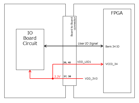
When using User IO at 3.3 V or when the IO Board consumes less than 0.3 A, VDD_3V3 can serve as the power supply.
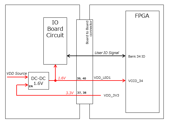
If User IO operates at 1.6 V or the IO Board’s current consumption is 0.3 A or more, use VDD_3V3 as the enable signal and provide power from the IO Board’s power supply.
Hardware Options and IO Connections
User IO Group 3 and WDOG_OUT signals can be routed to either TRCH or the FPGA, depending on hardware configuration. The connection configuration is fixed at shipment from Space Cubics and cannot be modified via software.
Please note that the signal power domain varies depending on whether it is connected to TRCH or the FPGA, so take care when designing the IO board.
| User IO | Endpoint when TRCH is selected | Endpoint when FPGA is selected |
|---|---|---|
UIO3_00 |
PIC16LF877 RD4/PSP4 |
FPGA IO_L23P_T3_12 (pin: Y15) |
UIO3_01 |
PIC16LF877 RD5/PSP5 |
FPGA IO_L23N_T3_12 (pin: AA15) |
UIO3_02 |
PIC16LF877 RD6/PSP6 |
FPGA IO_L24P_T3_12 (pin: W14) |
TRCH_UART_TX |
PIC16LF877 RC6/TX/CK |
FPGA IO_L24N_T3_12 (pin: W15) |
TRCH_UART_RX |
PIC16LF877 RC7/RX/DT |
FPGA IO_L1N_T0_12 (pin: AE26) |
WDOG_OUT |
PIC16LF877 RE0/AN5/RD |
FPGA IO_L16N_T2_12 (pin: AF18) |
-
Power domain
-
when TRCH is selected:
VDD_3V3_SYS -
when FPGA is selected:
VDD_3V3_IO
-
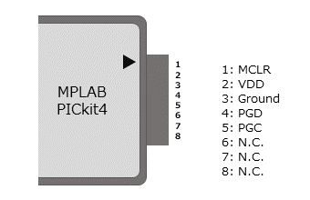
Debugger Connection
MPLAB PICkit4
TRCH software can be programmed using Microchip’s MPLAB and the PICkit4 debugger/programmer.
Connect MPLAB PICkit4 to the following pins on the OBC Module.
| MPLAB PICkit4 | OBC Module CON1 Pin No. |
|---|---|
1: MCLR |
51 |
2: VDD |
32 |
3: GND |
6, 15, 24, 29, 33, 48, 52, 57, 66, 75 |
4: PGD |
49 |
5: PGC |
50 |
6: N.C. |
unconnected |
7: N.C. |
unconnected |
8: N.C. |
unconnected |
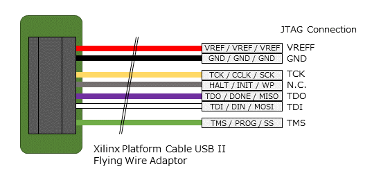
Platform Cable USB II
FPGA programming and in-circuit debugging can be performed using the Xilinx Platform Cable USB II.
Connect the USB II Platform Cable to the designated pins on the OBC module as shown below.
| Platform cable USB II | OBC Module CON1 Pin No. |
|---|---|
VREF |
OBC power signal (37, 38, etc.) |
GND |
6, 15, 24, 29, 33, 48, 52, 57, 66, 75 |
TCK |
53 |
HALT |
unconnected |
TDO |
54 |
TDI |
55 |
TMS |
56 |