Power Circuit Configuration
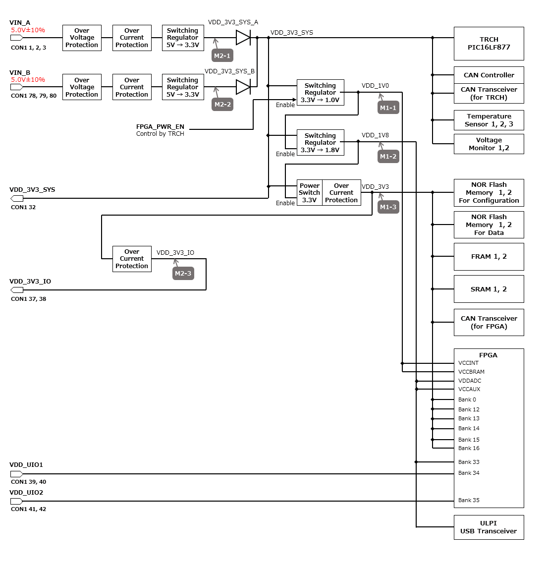
The power supply circuit configuration of the OBC module is shown below. Power supply inputs VIN_A (CON1 pins 1, 2, 3) and VIN_B (CON1 pins 78, 79, 80) operate redundantly, generating VDD_3V3_SYS_A and VDD_3V3_SYS_B independently. These two power lines are combined into VDD_3V3_SYS through ideal diodes and supply power to the TRCH and other components. Additionally, VDD_3V3_SYS is also provided externally via the IO board interface (CON1 pin 32). Since VDD_3V3_SYS is shared with internal circuits, its maximum current usage should not exceed 100 mA.
FPGA_PWR_EN activates each power IC, supplying power to internal circuits and external output pins as needed.
The generated power output nodes are equipped with current and voltage monitors, enabling power status monitoring from both TRCH and FPGA (M1-1, M1-2, M1-3, M2-1, M2-2, M2-3).
VDD_3V3_IO is supplied externally through the IO board interface (CON1 pins 37 and 38) and includes overcurrent protection rated at 300 mA.